3. DC circuits#
In this chapter the behavior of DC - or direct current - circuits are studied. A number of basic principles and analyses techniques will be covered that can also be applied to AC - or alternating current - circuits.
Basic electronic components#
Symbols#
The five basic elements for electronic circuits are resistance (\(R\)), coil (\(L\)), capacitor (\(C\)), voltage source (\(V\)) and current source (\(I\)) as shown in Fig. 4.
Fig. 4 also shows the symbols used for these basic elements.
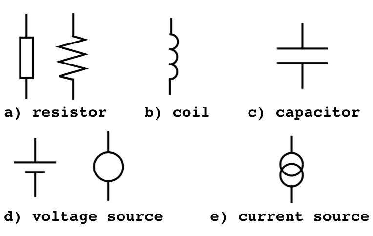
Fig. 4 Symbols for basic electronic elements#
Active and passive elements#
An active element is an element that can add net energy to a circuit. A passive element cannot add energy to a circuit, instead it receives energy from a circuit. Resistors, coils and capacitors are therefore passive elements, while voltage and current sources are active elements.
Linearity#
The three passive basic elements are linear. A resistor is linear because the potential difference across a resistor depends linearly on the current passing through it. A coil is linear because the potential difference across a coil depends linearly on change of current passing through it. A capacitor is linear because the change of potential difference across a capacitor depends linearly on the current through it. The linearity of passive elements simplifies the analysis of circuits strongly.
Kirchhoff’s laws#
Appendix B covers a number of basic laws, including Kirchhoff’s laws.
Network theorems#
Electronic circuits constructed of several resistors and sources quickly become complex. This section covers a number of circuit analysis techniques that simplify complex circuits.
Thévenin’s theorem#
Thévenin’s theorem offers the possibility to simplify complex circuits to a standard circuit with one voltage source and one resistor. The standard circuit is called the Thévenin equivalent circuit of the original complex circuit.
Thévenin’s theorem is defined as:
Any circuit with two terminals composed of resistors, voltage and/or current sources can be replaced by an ideal voltage source \(V\) and a resistor \(R\) in series.
The voltage \(V\) is called the Thévenin equivalent voltage \(V_{\rm Th}\) and resistor \(R\) the Thévenin equivalent resistor \(R_{\rm Th}\) (see Fig. 5).
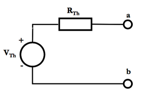
Fig. 5 Thévenin equivalent circuit#
\(V_{\rm Th}\) is equal to the open-circuit potential difference of the original circuit.
\(R_{\rm Th}\) is the resistance measured between terminals \(a\) and \(b\) when all voltage and current sources are replaced by their internal resistances.
From Fig. 5 it follows that \(R_{\rm Th}\) is given by:
where \(V_{\rm open}\) is the open-circuit potential difference and \(I_{\rm SC}\) is the short-circuit current obtained when terminals \(a\) and \(b\) are short cut.
Example Thévenin
Consider the circuit shown in Fig. 6.
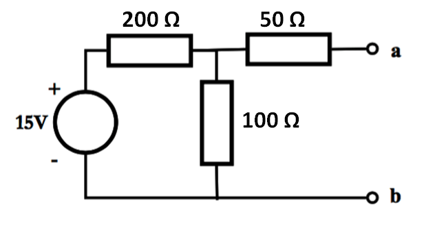
Fig. 6 Circuit example Thévenin#
Determination of \(V_{\rm Th}\):
\(V_{\rm Th}\) is the open-circuit potential difference between \(a\) and \(b\) in Fig. 6:
Determination of \(R_{\rm Th}\):
Assuming the voltage source is ideal, its resistance is 0 \(\Omega\). By replacing the voltage source by its internal resistance, \(R_{\rm Th}\) is obtained by determining the resistance between terminals \(a\) and \(b\) in Fig. 7:
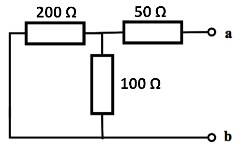
Fig. 7 Circuit to determine \(R_{\rm Th}\)#
This results in the Thévenin equivalent cicuit shown in Fig. 8:
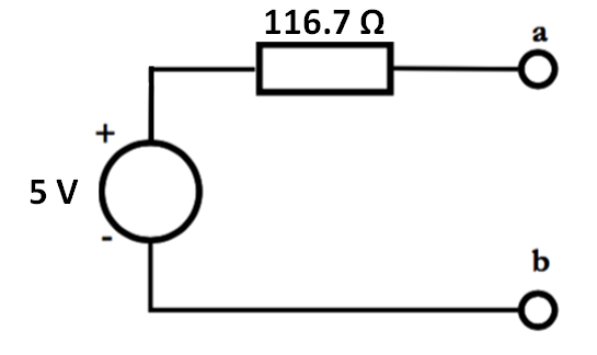
Fig. 8 Thévenin equivalent circuit#
Exercise 3.1
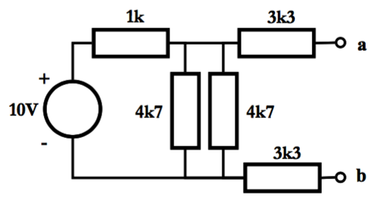
Fig. 9 Network with voltage source#
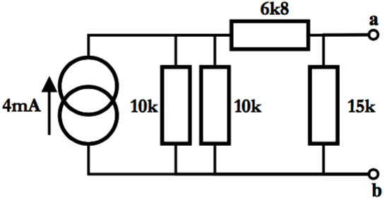
Fig. 10 Network with current source#

Open Mult 3.1a and Mult 3.1b and check your results.
Answer
(a) Since there is no load between terminals \(a\) and \(b\) \(V_{\rm Th}\) does not depend on the \(3k3\) loads. \(V_{\rm Th}\) is given by (see Fig. 11):
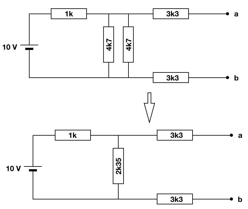
Fig. 11 Determination of \(V_{\rm Th}\)#
To calculate \(R_{\rm Th}\) the voltage source should be removed (see Fig. 12):
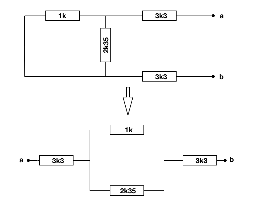
Fig. 12 Determination of \(R_{\rm Th}\)#
This results in Fig. 13.
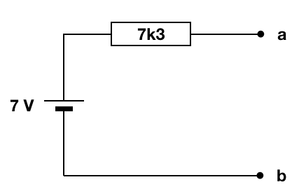
Fig. 13 Thévenin equivalent circuit#
(b) To determine \(V_{\rm Th}\) you first need to determine \(I_{\rm Th}\) (see Fig. 14):
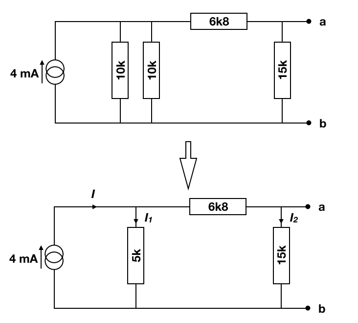
Fig. 14 Determination of \(V_{\rm Th}\)#
To determine \(R_{\rm Th}\) the current source should be removed by open terminals (see Fig. 15),
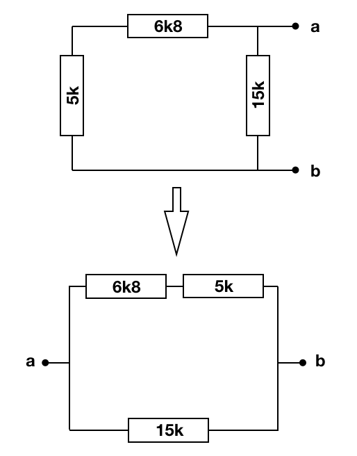
Fig. 15 Determination of \(R_{\rm Th}\)#
so:
This results in Fig. 16.
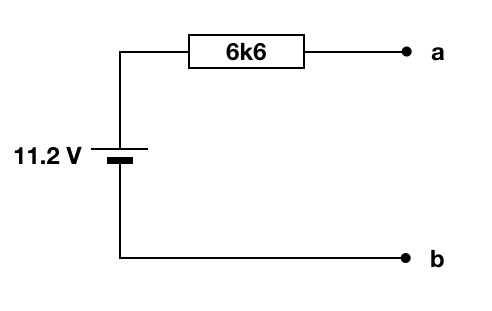
Fig. 16 Thévenin equivalent circuit#
The result in Multisim is the same (see Fig. 17):
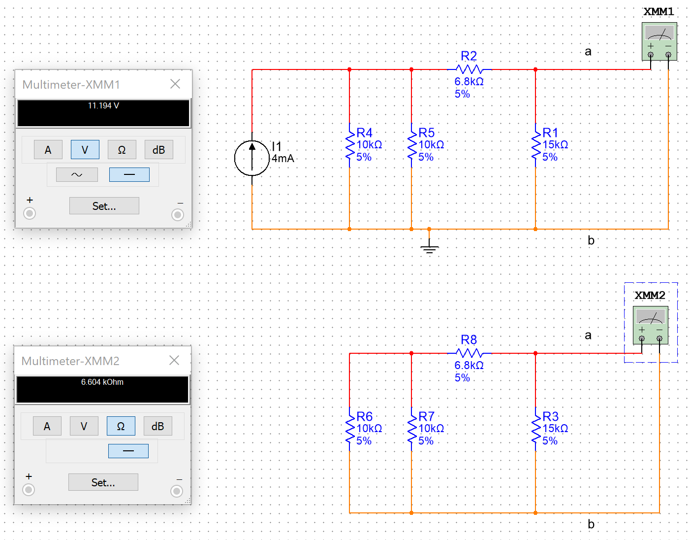
Fig. 17 The results of Mult 3.1b#
A second analysis technique to simplify circuits is Norton’s theorem. This theorem results in replacing any circuit for an ideal current source \(I\) in parallel with a resistor \(R\). In this course we will limit ourselves to Thévenin’s theorem.
Superposition theorem#
Some circuits contain more than one voltage and/or current source. In this situation the superposition theorem, derived from the linearity of basic elements, allows the determination of voltages across and currents through each of the sources separately. This is done by replacing sources by their internal resistance except for the source under consideration. For an ideal voltage source with internal resistance, replacing the source is the same as short cutting their terminals. For an ideal current source with infinite resistance replacing the source is the same as leaving their terminals open.
The superposition theorem is defined as:
The potential difference across a certain element in a circuit containing several sources can be obtained by determining the potential differences across that element due to each source, whereby all other sources are replaced by their internal resistances. The overall potential difference across the element is given by the algebraic sum of the separately determined potential differences.
For the current through a certain element a similar theorem applies.
Example Thévenin with two sources
Fig. 18 shows a circuit with a voltage and a current source.
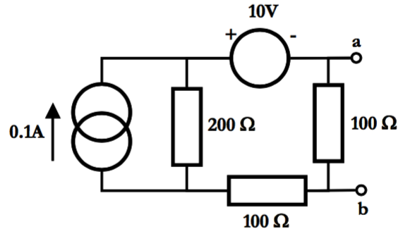
Fig. 18 Thévenin with two sources#
To find the Thévenin equivalent circuit the superposition theorem will be applied. The contributions of the voltage and current sources are calculated separately and then added.
To calculate the contribution of the current source the voltage source is short cut (i.e. replaced by its internal resistance). This results in the circuit shown in Fig. 19.
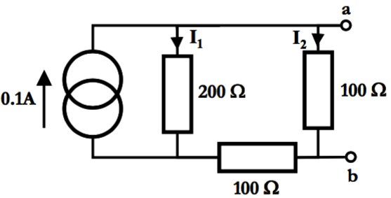
Fig. 19 Electronic circuit with voltage source eliminated#
The Thévenin equivalent voltage contribution of the current source is given by (check this!):
To calculate the contribution of the voltage source the current source terminals are kept open (replacement by its internal resistance). This results in the circuit shown in Fig. 20.
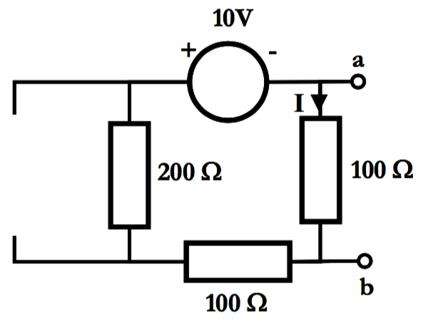
Fig. 20 Electronic circuit with current source eliminated#
Therefore (check this, pay attention to signs!):
To determine \(R_{\rm Th}\) both sources have to be replaced by their internal resistances. This results in the circuit shown in Fig. 21:
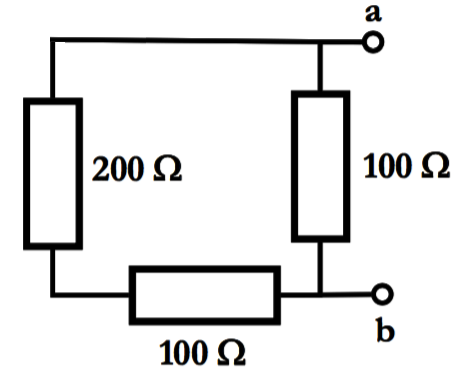
Fig. 21 Thévenin circuit with both source eliminated to determine \(R_{\rm Th}\)#
\(R_{\rm Th}\) is the resistance between terminals \(a\) and \(b\) and is given by:
Fig. 22 shows the Th{‘e}venin equivalent circuit.
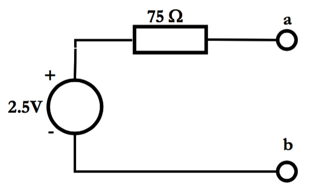
Fig. 22 The Thévenin equivalent circuit#
Exercise 3.2
Determine and draw the Thévenin equivalent circuit of Fig. 23.
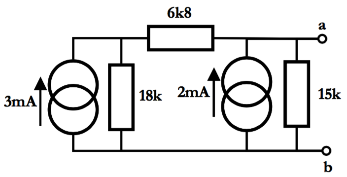
Fig. 23 Network with two current sources#
Open Mult 3.2 and check your results.
Answer
In order to determine \(V_{\rm Th}\) the circuit needs to be split up into two circuits with one current source each (see Fig. 24).
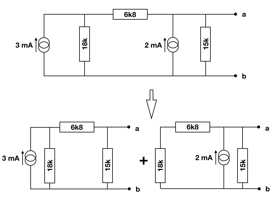
Fig. 24 Determination of \(V_{\rm Th}^{\rm 3 \; mA}\) and \(V_{\rm Th}^{\rm 2 \; mA}\)#
Then the \(V_{\rm Th}\) can be determined for each circuit.
So \(V_{\rm Th}\) is
To determine \(R_{\rm Th}\) the current sources should be removed by open terminals (see Fig. 25),
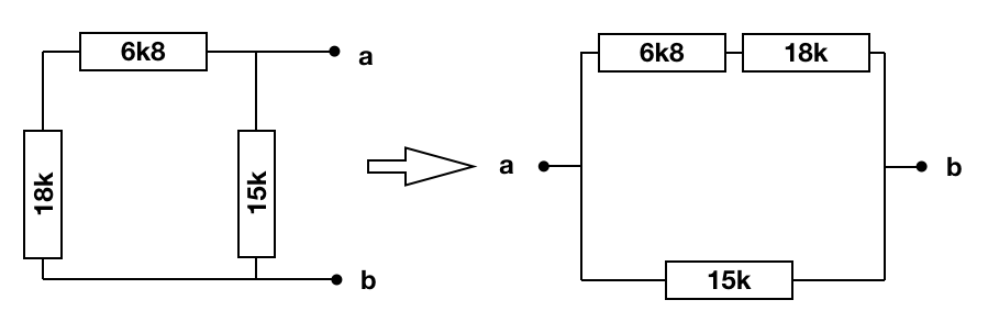
Fig. 25 Determination of \(R_{\rm Th}\)#
so:
This results in Fig. 26.
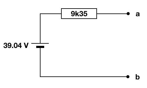
Fig. 26 Thévenin equivalent circuit#
The result in Multisim is the same (see Fig. 27):
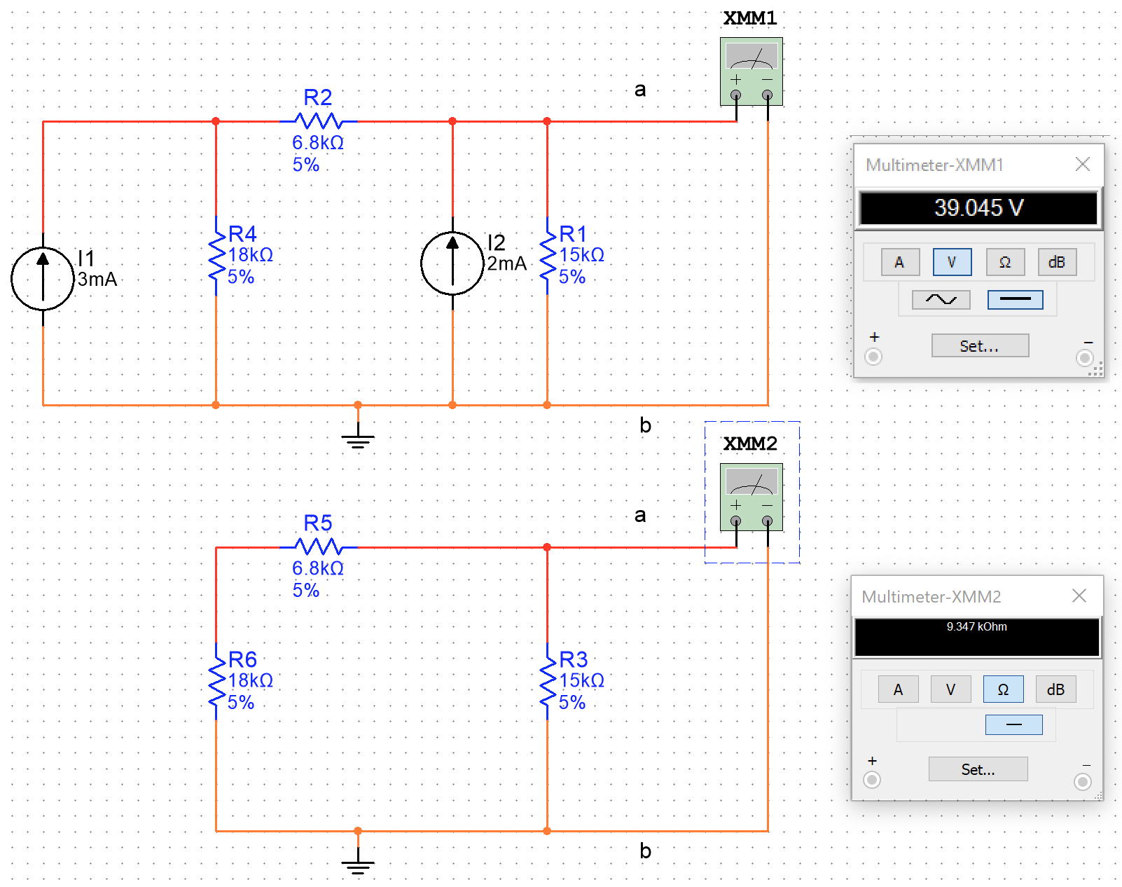
Fig. 27 The results of Mult 3.2#
Experimental determination of Thévenin and short cut values#
So far \(V_{\rm Th}\) and \(R_{\rm Th}\) have been determined by calculation, which is an option when the circuit is known in detail. When this is not the case and the circuit has to be treated as a ‘black box’ with two terminal, the \(V_{\rm Th}\) and \(R_{\rm Th}\) can be determined experimentally.
Determination of \(V_{\rm Th}\):
\(V_{\rm Th}\) simply is the open-circuit potential difference and can be measured when no load is connected to the circuit. However, it is important to use a measuring device with a high input impedance (see Input impedance) to ensure that the load on the circuit is minimal.
Determination of \(I_{\rm SC}\):
\(I_{\rm SC}\) is the short cut current. In general it is not wise to measure this current directly as it might damage the circuit. It is possible to measure \(I_{\rm SC}\) indirectly.
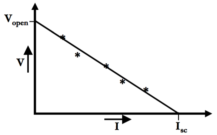
To do so load the circuit with a variable resistor \(R_{\rm v}\) as shown in Fig. 28. Measure the potential difference \(V_{\rm ab}\) and current \(I\) for several values of \(R_{\rm v}\) and display the results in a graph (see Fig. 29). Extrapolate the graph to determine \(I_{\rm SC}\) at \(V_{\rm ab} = 0\).
A simpler method is to vary \(R_{\rm v}\) until \(V_{\rm ab} = \frac{1}{2} V^{\rm open}_{\rm ab}\). For this resistance value \(R_{\rm v} = R_{\rm Th}\) (check this!). Using eqn. (2) \(I_{\rm SC}\) can be obtained.
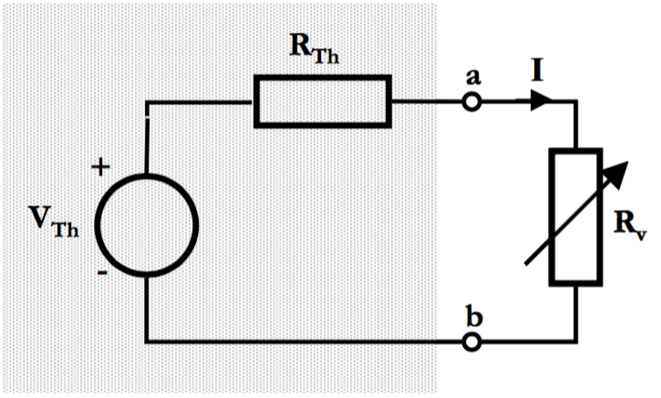
Fig. 28 Experimental determination of \(I_{\rm SC}\)#
Input impedance#
A voltage source connected to the input terminals of a circuit usually results in a current running through the circuit. The strength of the current depends on the input impedance \(R_{\rm i}\) of the circuit. Similar to the Thévenin equivalent circuit, which is used to describe the output of a circuit, the behavior of the input of a circuit may be described by using an equivalent input circuit, as shown in Fig. 30.
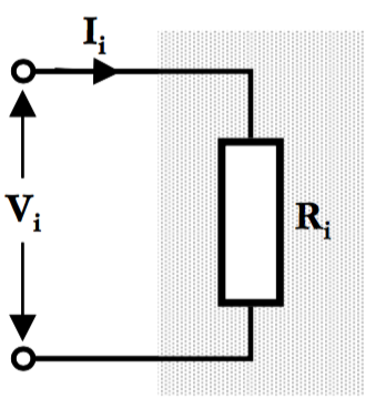
Fig. 30 Equivalent input circuit#
\(R_{\rm i}\) is given by
When details on the circuit are available \(V_{\rm i}\) and \(I_{\rm i}\), and therefore \(R_{\rm i}\) can be calculated. If this is not the case \(R_{\rm i}\) can be determined experimentally in a similar way as the experimental determination of \(R_{\rm Th}\) (see Experimental determination of Thévenin and short cut values):
Connect a variable resistor and a voltage source to the circuit as shown in Fig. 31.
Measure the output potential difference \(V_{\rm s}\) of the voltage source and the input potential difference \(V_{\rm i}\) of the test circuit. Vary \(R_{\rm v}\) until \(V_{\rm i} = \frac{1}{2} V_{\rm s}\). Then \(R_{\rm i} = R_{\rm v}\) (check this!).
Note that this method does not depend on the value of \(R_{\rm s}\). This is due to measuring \(V_{\rm s}\) rather than \(V_{\rm open}\).
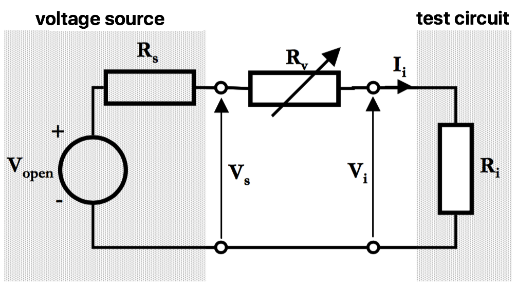
Fig. 31 Experimental determination of input impedance#
Amplification#
Type of amplification#
Different kinds of amplifiers can be classified.
First, amplifiers for DC signals (DC amplifiers) and AC signals (AC amplifiers) are distinguished.
Second, amplifiers are distinguished according to the type of signal which requires amplification. If the input and output signals are potential differences we refer to a voltage amplifier, if they are currents we refer to a current amplifier. If the input signal is a potential difference and the output signal a current we refer to a voltage to current converter, and in the reverse situation to a current to voltage converter. When the objective is to increase the power (rather than the potential difference or current), as is the case in an audio amplifier, we refer to a power amplifier.
Amplification can be considered as a transfer function \(A\) (see Transfer function), which signifies the relation between the output signal \(y\) and the input signal \(x\):
For voltage amplification eqn.(\ref{tf}) turns into:
for current amplification:
and for power amplification:
where \(V_{\rm in}\), \(I_{\rm in}\) and \(P_{\rm in}\) are the input potential difference, current and power, and \(V_{\rm out}\), \(I_{\rm out}\) and \(P_{\rm out}\) the output potential difference, current and power, respectively.
Equivalent circuit amplifier#
An amplifier is a circuit with an input and output. The input may be replaced by an effective input impedance (see Input impedance) and the output can considered as a voltage source en hence can be simplified using Thévenin’s theorem (see Thévenin’s theorem).
Fig. 32 shows the equivalent circuit of a voltage amplifier.
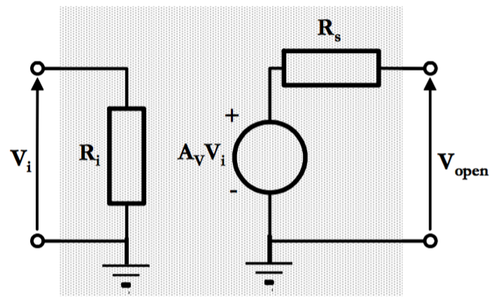
Fig. 32 Equivalent circuit of a voltage amplifier#
\(V_{\rm i}\) is the input potential difference, \(R_{\rm i}\) the effective input impedance, \(A_{\rm v}V_{\rm i}\) the equivalent Thévenin voltage source, \(A_{\rm v}\) the voltage amplification, and \(R_{\rm s}\) the Thévenin output impedance. Note that the Thévenin voltage source is not an actual voltage source, but rather a voltage source dependent on the input potential difference.
Matching#
When two electronic systems are interconnected it is important that the information from one system is transferred to the other in the correct manner.
When a potential difference is the information carrier the potential difference should be transferred with minimal change. In other words, the output potential difference of the first system after connection to the second system should differ as little as possible from the open output potential difference of the first system.
Fig. 33 shows a schematic, where system 1 is a voltage source with an open potential difference \(V_{\rm open}\) and output impedance \(R_{\rm s}\) and system 2 is characterized by the input impedance \(R_{\rm i}\).
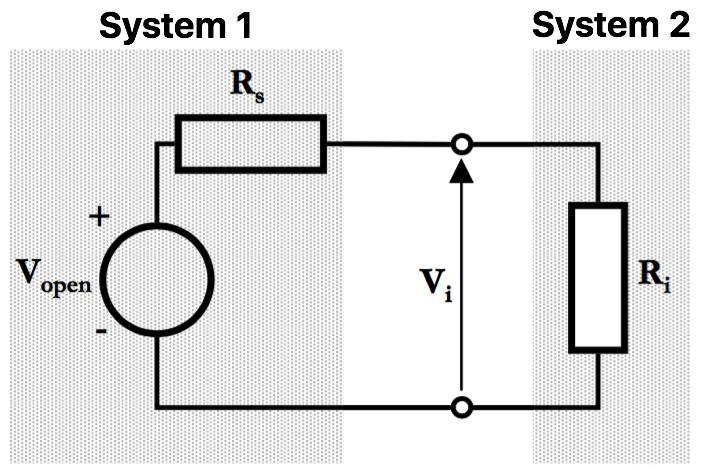
Fig. 33 Example of connecting voltage source with a second system#
The input potential difference of system 2 is given by:
From eqn. (22) it follows that the voltage transfer improves as the input impedance \(R_{\rm i}\) of system 2 increases.
When a current is the information carrier the input current of the second system should differ as little as possible from the short cut current of the first system.
Fig. 34 shows a schematic, where system 1 is a current source \(I\) with an output impedance \(R_{\rm s}\) and system 2 is characterized by the input impedance \(R_{\rm i}\).
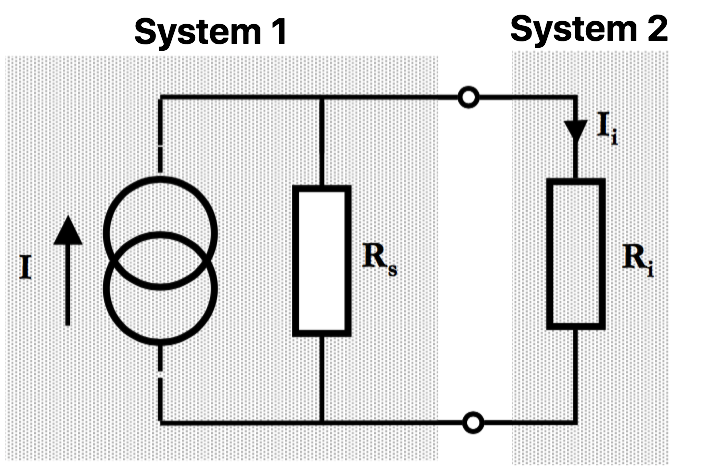
Fig. 34 Example of connecting a current source with a second system#
The input current of system 2 is given by:
From eqn. (23) it follows that the current transfer improves as the input impedance \(R_{\rm i}\) of system 2 decreases.
So:
\(R_{\rm i}\) large: good voltage transfer, poor current transfer
\(R_{\rm i}\) small: good current transfer, poor voltage transfer
In many cases, e.g. when connecting a loudspeaker to an audio amplifier, the objective is not to facilitate an optimal voltage or current transfer, but to maximize the power transfer. What is the optimal value of \(R_{\rm i}\) in that case? The power transfer at \(R_{\rm i} = 0\) and \(R_{\rm i} = \infty\) is 0 (check this!).
Assume that in Fig. 33 system 1 represents an audio amplifier and system 2 a loudspeaker. The power transferred to the loudspeaker is (using eqn. (22)):
To find the maximum power transfer the derivative of \(P\) with respect to \(R_{\rm i}\) is taken:
The maximum power transfer is obtained when eqn. (25) is set to 0. Check that this is the case for \(R_{\rm i} = R_{\rm s}\).
This in fact shows that half of the power is dissipated in the output impedance \(R_{\rm s}\) of the amplifier and the other half in the input impedance of the loudspeaker.
Substitution of \(R_{\rm i} = R_{\rm s}\) into eqn. (24) give the maximum power transfer:
Power amplification often is expressed in decibel (dB). Appendix C gives some examples of logarithmic forms.
Application of a network#
The Wheatstone bridge#
The Wheatstone bridge is an example of a network with a voltage source. The general configuration is shown in Fig. 35. This circuit is used to measure small changes in resistances, or to measure resistance values accurately.
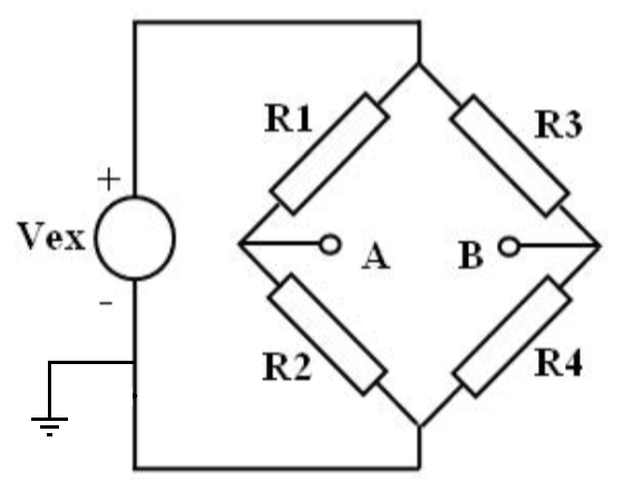
Fig. 35 The Wheatstone bridge#
Physical quantities, like temperature, pressure and deformation of materials, are usually measured using sensors dependent on resistance. For example, for temperature measurements NTC resistors are used, which at room temperature have a value of 2 k\(\Omega\), with a temperature coëfficient of 1 \(\Omega / ^{\rm o}\)C. Assume that we want to measure a temperature change of 1 \(^{\rm o}\)C with an accuracy of 5%, then changes in resistance of about 0.05 \(\Omega\) should be measured with a range of 2 k\(\Omega\). With an ordinary multimeter this is very hard to realize.
One way of do this is by using a Wheatstone bridge. A Wheatstone bridge is constructed using two parallel voltage dividers \(R_1 / R_2\) and \(R_3 / R_4\).
With the right selection of resistors the bridge can be balanced, which results in a potential difference \(V_{\rm AB} = 0 \, {\rm V}\). In that case:
Small changes in one of the resistors results in small potential differences between \(A\) and \(B\). For the temperature measurement \(R_1\) may be replaced by the NTC sensor, with \(R_2 = R_3 = R_4 = 2 \, {\rm k} \Omega\). At room temperature the bridge is balanced. Small temperature changes will result in small changes in \(V_{\rm AB}\).
Exercise 3.3
Derive the relations for \(V_{\rm AB}\) as a function of \(V_{\rm ex}\), \(R_1\), \(R_2\), \(R_3\) and \(R_4\).
Open Mult 3.3 and check for a number of values of \(R_1\) the open potential differences \(V_{\rm AB}\).
Answer
Fig. 36 tells us that
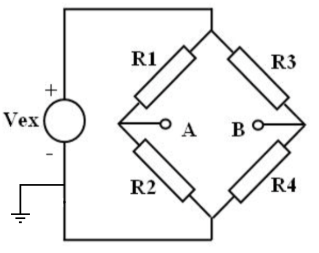
Fig. 36 The Wheatstone bridge#
So \(V_{\rm AB}\) is given by
This is confirmed by Multisim: with \(R_2 = R_3 = R_4 = 10 \; {\rm k} \Omega\) and varying \(R_1\) from 9995 to 10005 \(\Omega\) results in voltage steps of 250 \(\mu\)V (see Fig. 37).
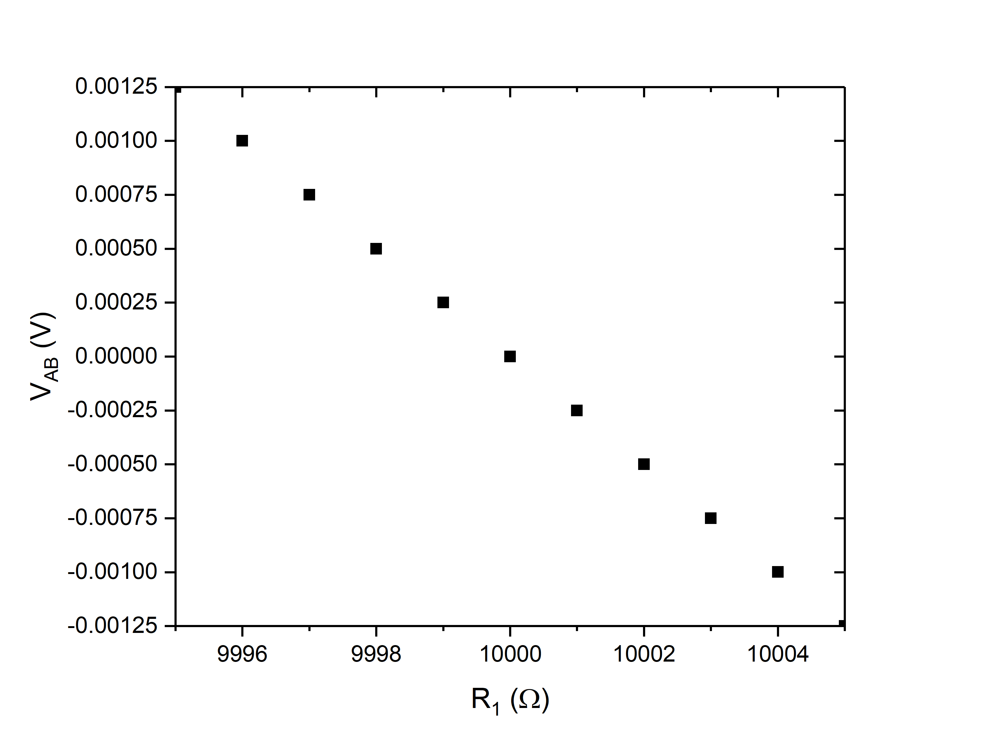
Fig. 37 Results of the Wheatstone bridge measurement#
Lab exercises#
Before you start on the lab exercises read the section Problem solving (Problem solving) and Reporting (Reporting of lab exercises).
Exercise 3.4

The terminals \(A\) and \(B\) of the voltage divider shown in Fig. 38 can be considered terminals of a new voltage source with an internal resistance \(R_{\rm i}\).
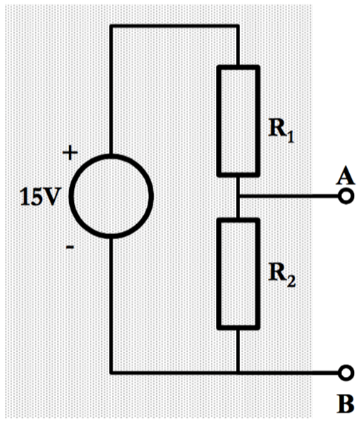
Fig. 38 Voltage divider#
Design the circuit shown in Fig. 38 using Multisim in such a way that \(V_{\rm AB} \approx 0.5 \, {\rm V}\), while the power \(P\) of the voltage source of 15 V (\(R_{\rm i \, (15V)} = 5 \, \Omega\)) does not exceed 150 mW. (Two conditions!)
Construct the circuit.
Determine the internal resistance \(R_{\rm i}\) of the new voltage source by measuring \(V_{\rm AB}\) for various loads \(R_{\rm load}\) (see Fig. 39).
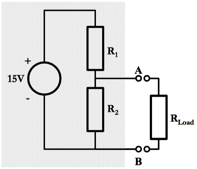
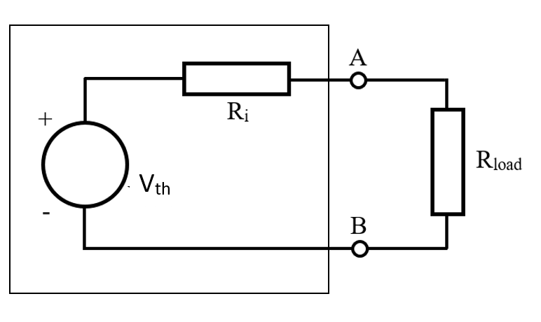
Fig. 39 New voltage divider with \(R_{\rm load}\)#
Plot your data such that \(R_{\rm i}\) can be determined from the graph.
Compare the experimentally determined \(R_{\rm i}\) with the calculated value. Give an explanation for any differences.
Exercise 3.5
An NTC has a resistance of \(R_{\rm ref} = 2 \, {\rm k} \Omega\) at \(T = 20 \, ^{\rm o} {\rm C}\) and a temperature coefficient of \( 1 \, \Omega / ^{\rm o} {\rm C}\). Because it is hard to create different stable temperatures, the NTC will be simulated by a variable resistor.
Construct a Wheatstone bridge, as shown in Fig. 35, to measure temperatures close to room temperature. Use a variable resistor for \(R_1\) and \(V_{\rm ex} = 15 \, {\rm V}\).
Derive a relation for \(V_{\rm AB}\) as a function of \(\Delta R\), \(R\) and \(V_{\rm ex}\) for the special case that NTC \(R_1 = \Delta R + R\) and \(R_2 = R_3 = R_4 = R\).
Check this relation experimentally for a number of measurements. (For \(\Delta R \ll R\).) Discuss your results.
Calculate \(V_{\rm AB}\) per \(^{\rm o} {\rm C}\), and compare this value with the one experimentally determined.